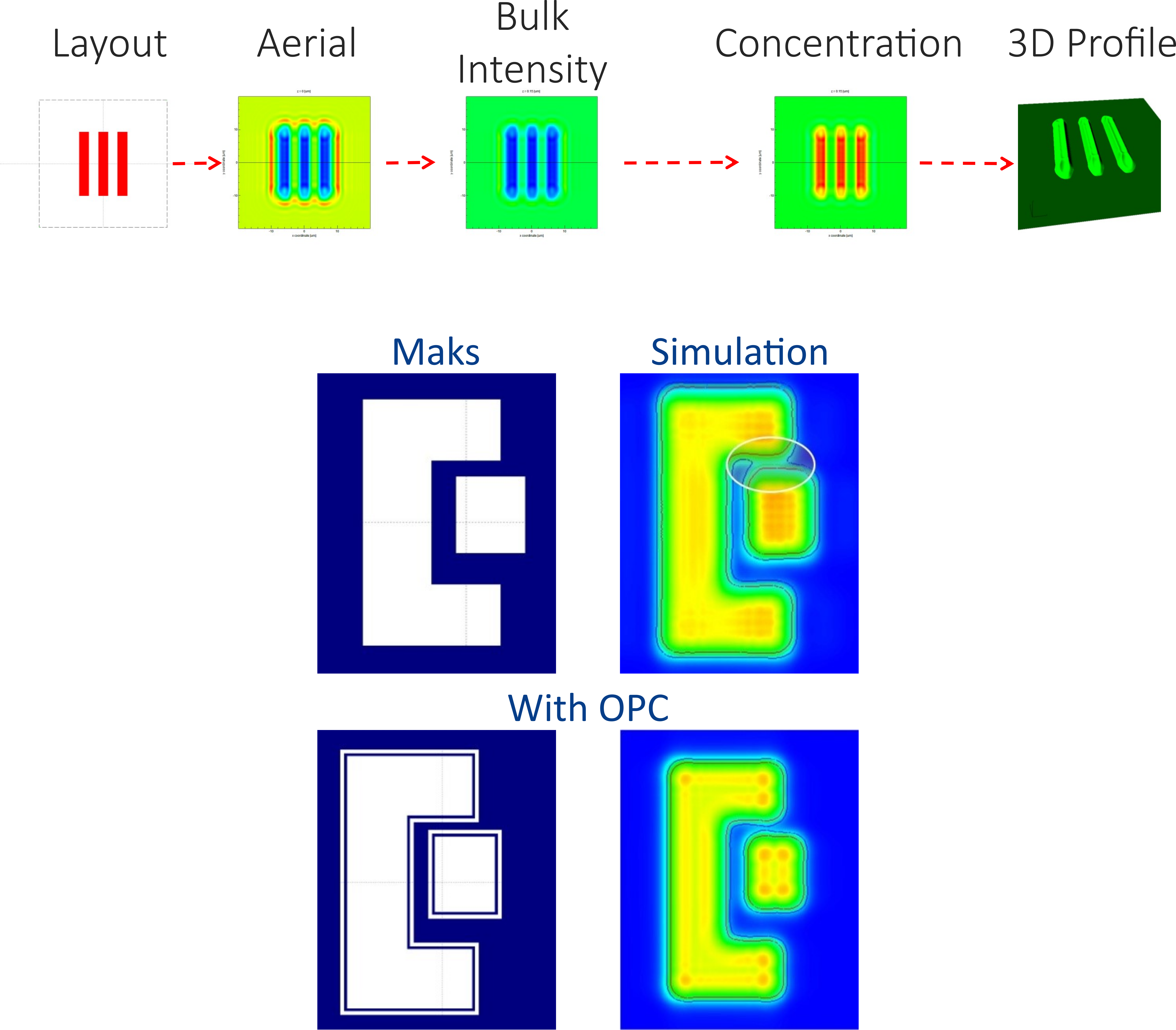
LAB simulation methods and Optical Proximity Correction in Lithography
Motivation:
The simulation of lithographic processes involves many factors as optical properties of materials, source angle of incidence, diffraction, and more. The accuracy of the results highly relies on the models used and the parameters for calibration. However, implementation of physical models is not an easy task. Additionally, once a simulation is set, layout modifications provide extra means to optimise the outcome of a design. Therefore, too many factors influence devices optimisation.
Solution:
LAB offers the desired simulation platform for lithography. The intensity and resist images are simulated fast, and with high accuracy. The use of layout operations such as Bias, Transform, and Boolean operations makes it easy to modify a layout optimising shape, size, and position of feature for Optical Proximity Correction. The integrated layout editor allows the semi-automated optimisation of the layout for the best match of the lithography result to the intended design. Changing different parameters allows the simulation of hundreds of different conditions in hours or even in minutes. Moreover, the process window analysis tool makes it easy to analyse the printability of the selected pattern.

